
A seed gives the silicon a repeating structure
The pull is not simply a way to make a solid rod. It gives silicon atoms a template to follow. A small seed crystal touches the molten silicon; as it is drawn upward, atoms leaving the melt join the seed’s orderly pattern. That continuous atomic arrangement is called a single crystal. Unlike a solid assembled from many differently oriented grains, it has no internal grain boundaries interrupting the pattern.
That order matters because a chip depends on controlling how electrical charge moves through silicon. Even small variations in the material can make that behavior harder to predict. Producers can also add tiny amounts of other elements to the melt to adjust the silicon’s electrical properties—a step called doping.
Growth is a balancing act
The seed and the growing crystal are rotated, while the pull speed and temperature are carefully managed. Silicon must solidify at the boundary between the melt and the crystal: too much heat or too little can disrupt growth, while uneven cooling can create stresses or defects. The growing cylinder, known as an ingot, must also reach a consistent width so it can be turned into wafers with usable area.
The process therefore controls more than shape. It aims to preserve the crystal’s structure and desired electrical characteristics throughout a large volume of material.
Turning the ingot into a working surface
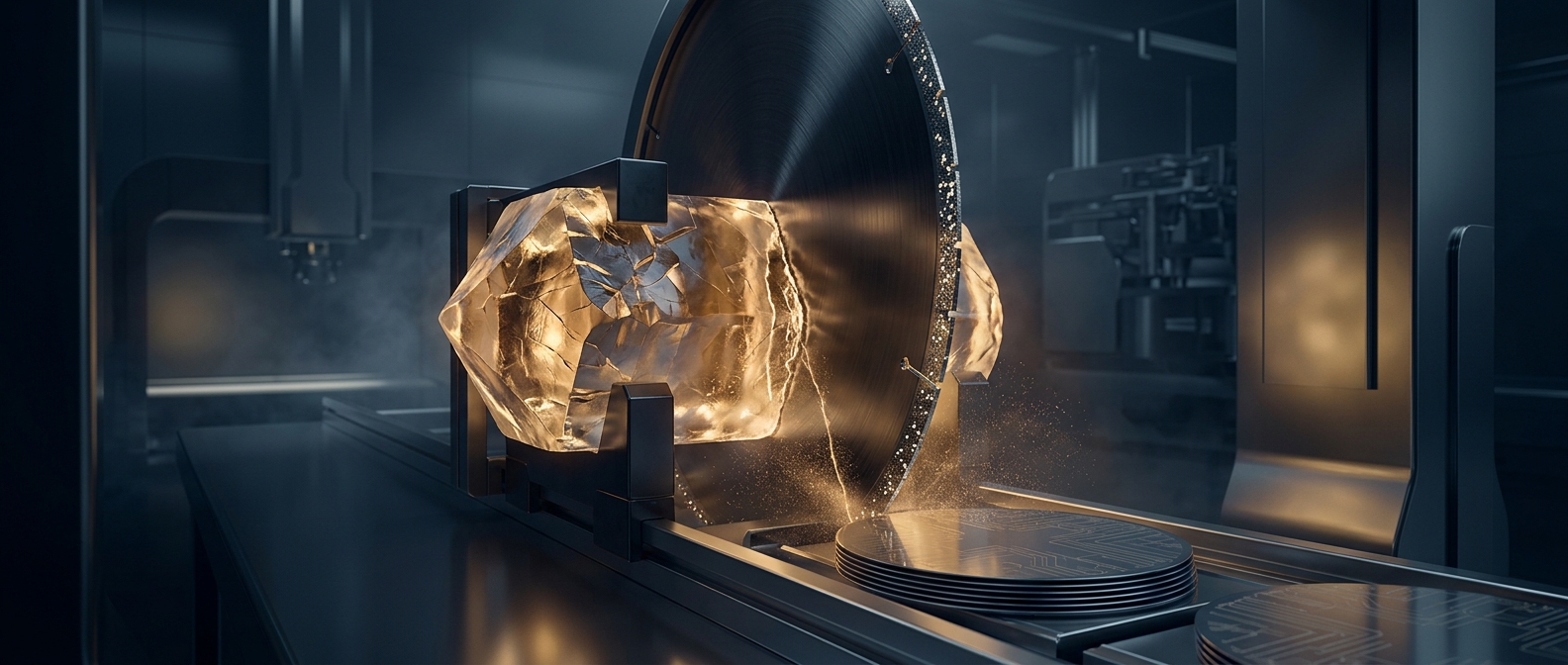
After growth, the ingot is cut into thin disks. Cutting leaves microscopic damage and an uneven surface, so wafers are ground and polished before chip-making begins. Later steps build intricate circuits on the wafer’s surface, but those patterns depend on having a flat, clean foundation.
A single crystal can supply many wafers, and each wafer can hold many chip designs. The quality of that first carefully grown structure is carried forward into every one of them.