Turning a wafer into one computing surface
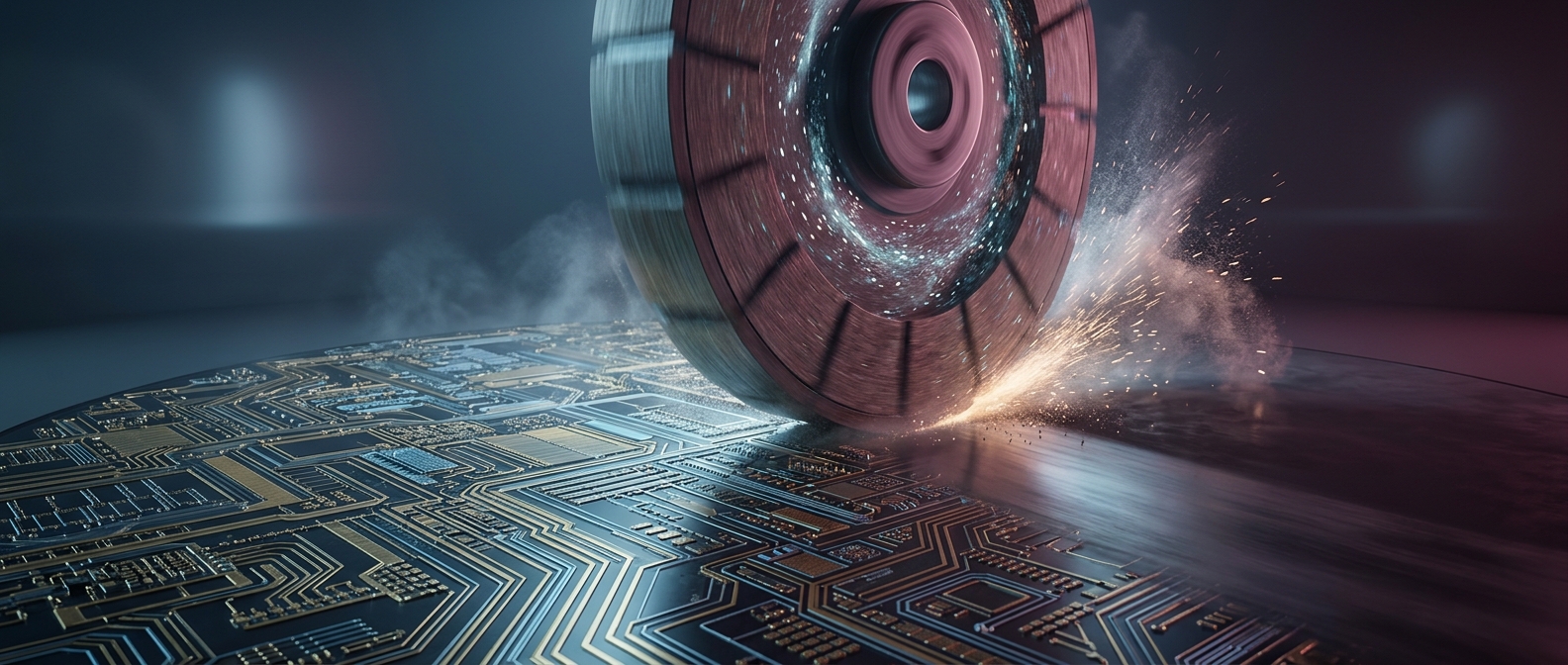
A silicon wafer is the round disc on which many chips are manufactured. Ordinarily, the finished wafer is cut into individual chips, and those chips are packaged and connected on a circuit board. Cerebras instead keeps a vast section of the wafer intact as one processor. That changes the scale of the design: the computing cores and the pathways linking them can be arranged across a continuous piece of silicon.
Why keeping the silicon connected matters
In a conventional AI system, a model’s data may have to move between separate processor chips. It travels through connections outside each chip, adding communication delays and consuming energy. On a wafer-scale processor, neighboring cores can exchange data through on-silicon links. For workloads that repeatedly pass information among many parts of a model, that can reduce the cost of moving data and help keep computation close to where it is needed.
The benefit is not simply that a larger chip can hold more cores. The physical route between those cores matters: shorter, more direct connections can make a large group of processors function more like a tightly coordinated system.
The manufacturing problem behind the idea
A wafer is not guaranteed to be perfect. A flaw that would make a small chip unusable could land somewhere inside a processor this large. Wafer-scale designs therefore need ways to identify defective regions and keep them from disrupting the rest of the device, using working resources around the flaw where the architecture allows. They also face the practical challenge of delivering power and removing heat across a much larger area.
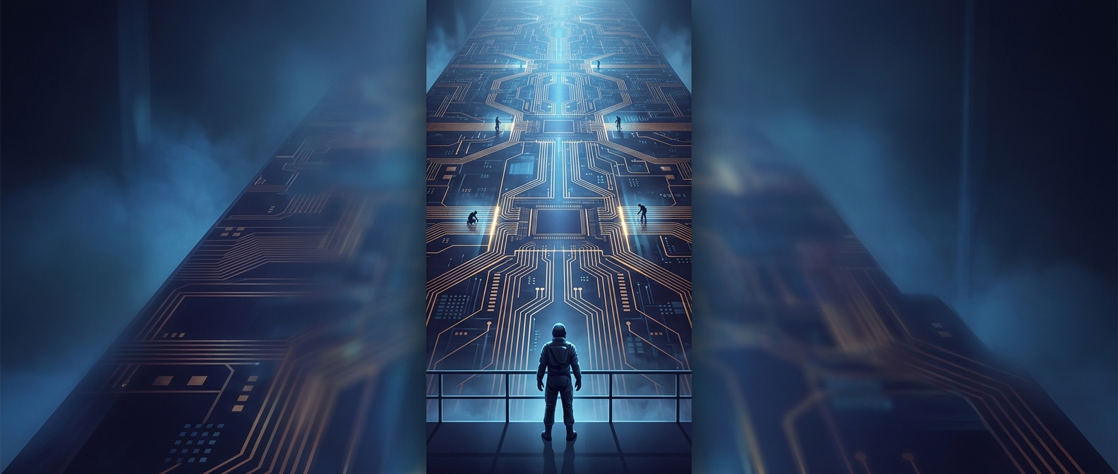
That tradeoff is central to the design: preserve the fast communication of a single silicon surface while making a wafer-sized processor manufacturable and manageable. The striking consequence is that an AI computer can treat a broad field of on-wafer cores as one connected workspace, rather than repeatedly handing data from chip to chip.