The screen is assembled in batches, not one light at a time
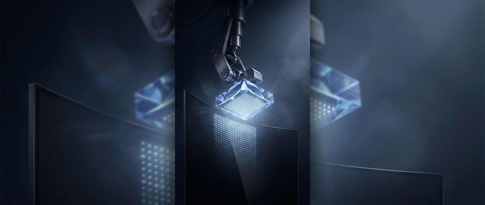
A microLED display is built from an enormous number of microscopic light-emitting diodes, or LEDs. Each one must end up at a precise spot on a display backplane—the circuit layer that controls which lights turn on and how brightly. Moving every diode individually would make assembly painfully slow, so manufacturers try to transfer many at once.
One approach uses an elastomeric stamp, a soft, slightly flexible surface. It contacts a group of LEDs on a source wafer, picks them up, then presses them onto the backplane. The stamp’s grip can change with the way it touches and lifts, allowing it to collect and release the tiny components in sequence.
Why a soft stamp or a laser helps
A laser-based process uses light to free LEDs from their original substrate, the material on which they were made. The released components can then be transferred to the display. Both methods replace a long series of individual placements with operations that handle groups of parts, though the exact process depends on the design and manufacturer.
The difficulty is that “many at once” also means many chances for error at once. The LEDs must land in the right locations, remain intact, and make reliable electrical connections. A small placement or connection problem can leave a visible dark or faulty spot. Manufacturers therefore have to balance speed against precision and check the assembled display for defects.
That tradeoff is central to making large microLED screens practical: the goal is not merely to manufacture tiny lights, but to move them into a working display in vast numbers without sacrificing accuracy.